- October 08, 2025
Summarize with AI
Not enough time? Get the key points instantly.
Get summary:
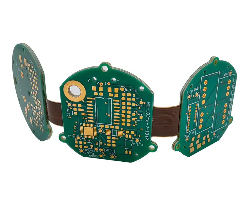
What Our Hardware Leaders Says About High Speed PCB Design ?
High speed PCB design is different scenario because there is engineering shifts from “connecting components” to controlling physics when comes to high speed.
At lower frequencies, a PCB is forgiving. Signals behave predictably, layouts are flexible, and small mistakes rarely break functionality. But as speeds increase, your PCB becomes a high-frequency system, not just a circuit board.
That’s when things start going wrong including unexpected noise, failed tests, signal distortion, and costly redesigns.
This guide walks you through why high speed PCB design needs expert guidelines, what makes it complex, and how to approach it step by step from schematic to gerber which help you to avoid costly respins.
Why High Speed PCB Design Needs Expert Guidelines
One of the biggest misconceptions is that high speed PCB design is not tricky as compare to standard PCB design.
At high speeds, signals behave like electromagnetic waves traveling through transmission lines. This means every trace, via, and plane directly affects signal behavior.
Without proper guidelines, teams run into problems that are hard to predict and even harder to debug.
The common reasons why high speed PCB needs expert opinion
Most teams don’t struggle at the design stage. They struggle after the first prototype.
It worked in simulation
Design tools and simulations don’t always capture real-world effects like parasitics, material inconsistencies, and layout imperfections.Repeated PCB respins
A minor impedance mismatch or poor routing decision can require a full redesign, costing weeks of time and significant budget.Signal integrity issues
Reflections, ringing, attenuation, and crosstalk start appearing as speeds increase.EMI/EMC failures
Boards fail compliance testing because electromagnetic emissions weren’t controlled early in the design.Debugging becomes reactive
Instead of designing confidently, teams spend time diagnosing invisible problems using oscilloscopes and guesswork.
These challenges are exactly why structured high speed PCB design guidelines are critical.
What Makes High Speed PCB Design so Complicated
The complexity doesn’t come from one factor. It comes from how everything interacts.
At high speeds:
Traces behave like transmission lines
Signal return paths become critical
Timing differences affect functionality
Power delivery impacts signal quality
A small change in one area can create unexpected problems in another.
For example, increasing trace length doesn’t just delay a signal.
It can also change impedance, introduce reflections, and affect synchronization.
This interconnected behavior is what makes high speed digital design far more complex than traditional PCB design.
Key Factors to Consider in High Speed PCB Design
To avoid failures, you need to think about the entire system - from schematic to manufacturing.
Stack-up planning
Everything starts with the PCB stack-up.
This includes:
Number of layers
Placement of signal and ground planes
Controlled impedance layers
A well-defined stack-up ensures consistent impedance and reliable signal paths. If this is wrong, no amount of routing optimization can fix it later.
Signal integrity
In high speed PCB design, signal integrity determines whether your board works reliably.
Important aspects include:
Controlled impedance
Proper termination
Minimizing reflections
Managing crosstalk
Ignoring signal integrity leads to unstable performance and intermittent failures.
Component placement
Placement is not just about fitting components on the board.
It defines how easily signals can be routed and how clean those paths will be.
Good placement practices include:
Keeping high-speed paths short
Placing related components close together
Avoiding unnecessary vias
Poor placement increases routing complexity and degrades signal quality.
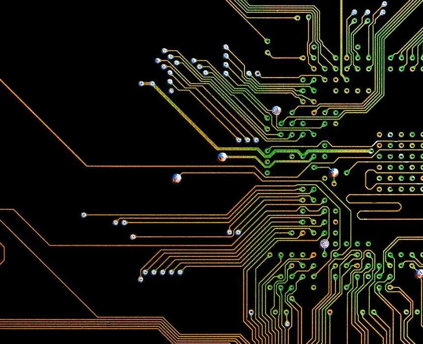
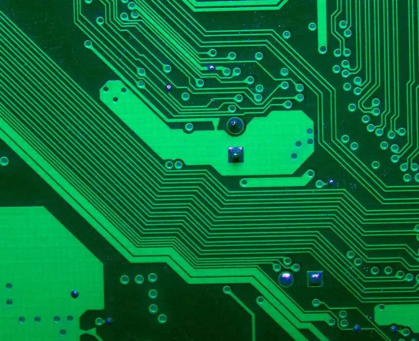
Routing
Routing in high speed PCB design is highly disciplined.
You need to:
Maintain consistent trace width
Avoid sharp corners
Minimize stubs
Match lengths for differential pairs
Routing is where most signal integrity issues are introduced.
Power integrity
Power delivery directly affects signal performance. Noise in power lines can corrupt signals, even if routing is perfect.
Key considerations include:
Proper decoupling capacitor placement
Solid power and ground planes
Minimizing voltage fluctuations
Many signal issues are actually power integrity problems in disguise.
Grounding and return paths
Every signal has a return path. If that path is disrupted, it creates noise, EMI, and signal distortion.
Best practices include:
Continuous ground planes
Avoiding splits under high-speed signals
Ensuring clear return paths
This is one of the most overlooked aspects of high speed PCB design.
EMI/EMC
Electromagnetic interference is not something you fix at the end. It must be designed for from the beginning.
This involves:
Reducing loop areas
Controlling signal transitions
Shielding sensitive signals
Ignoring EMI early often leads to compliance failures later.
Design for Manufacturability (DFM)
Even a technically perfect design can fail if it’s difficult to manufacture.
You need to:
Follow fabrication constraints
Avoid extreme tolerances unless necessary
Align design with manufacturer capabilities
This ensures your design can be built consistently and reliably.
Step-by-step High Speed PCB Design Process
A structured approach helps reduce errors and improve outcomes.
Step 1: Define requirements clearly
Every successful high speed PCB design begins with clarity.
You need to understand what your board is expected to handle—not just functionally, but electrically. High-speed signals behave differently depending on frequency, timing, and environment.
At this stage define
Signal speeds and interfaces (DDR, PCIe, USB, etc.)
Timing constraints and allowable skew
Target impedance requirements
EMI/EMC compliance expectations
This defines the design constraints.
Step 2: Plan the stack-up
A well-defined stack-up ensures that your impedance, return paths, and signal behavior are predictable in the real world, not just in simulation.
Work with your PCB fabricator to finalize:
Number of layers and their arrangement
Dielectric materials and thickness
Controlled impedance layers
Ground and power plane distribution
A poor stack-up forces compromises in routing and signal integrity. A strong stack-up makes the rest of the design easier and more reliable.
Step 3: Create the schematic with intent
Instead of just connecting components logically, think about how signals will physically flow across the board.
Focus on:
Logical grouping of related components
Clean signal paths without unnecessary branching
Placement of termination and filtering components with layout in mind
A well-thought-out schematic reduces layout complexity significantly. A messy schematic creates routing challenges that degrade performance.
Step 4: Optimize component placement
Good placement minimizes routing complexity and preserves signal integrity. Poor placement forces long traces, extra vias, and broken return paths.
While placing components, ensure:
Critical components are placed based on signal flow
High-speed paths are kept short and direct
Related components are grouped closely
Layer transitions (vias) are minimized wherever possible
Think of placement as pre-routing. If placement is right, routing becomes controlled.
Step 5: Route critical signals first
These include clocks, differential pairs, and high-speed interfaces. These signals are highly sensitive to impedance changes, noise, and discontinuities.
While routing them, maintain strict discipline:
Use controlled impedance trace widths
Maintain consistent spacing in differential pairs
Avoid sharp bends and unnecessary stubs
Match lengths where timing is critical
Once these signals are routed correctly, you protect the core functionality of your design.
Step 6: Complete general routing
After critical signals are secured, move to the rest of the routing. Even though these signals are less sensitive, they still need to follow design rules to avoid introducing noise or interference.
During this phase:
Follow spacing and clearance rules consistently
Avoid routing over split planes
Maintain clean return paths for all signals
Prevent congestion that could affect signal integrity
Step 7: Perform simulations and validation
At high speeds, assumptions are risky. Simulation and analysis help you catch issues early.
Run checks for:
Signal integrity (reflections, crosstalk, losses)
Power integrity (voltage stability, noise)
EMI/EMC risks
Step 8: Generate Gerber files
Errors at this stage can lead to fabrication issues even if your design is perfect.
Ensure:
All layers are correctly defined and labeled
Drill files and via details are accurate
Stack-up and impedance details are documented
Fabrication notes are clear and complete
A careful handoff to manufacturing reduces surprises later.
Step 9: Prototype and test
Once prototypes are built, test them thoroughly to ensure they behave as expected under actual conditions.
Focus on:
Signal quality and waveform integrity
Noise levels and interference
Compliance with EMI/EMC standards
Use these results to refine the design if needed.
How Our Hardware Team Can Guide You in High Speed PCB Design
CoreFragment Technologies helps you to avoid delay, respins and unstable designs. We work as hardware partner in each stage of PCB design instead of just another design vendor.
We work in these areas to make your hardware compliant, scalable and working.
Requirements and Risk Definition - We help your team to define system requirements, interface constraints and risk areas in your product. Our design approach revolves around this factors.
Stack up and Schematic - We help you with manufacturing ready stack up, schematic review, proper planning for routing and signal flow.
Built in EMI and reliability thinking - We guide you through how EMI can be controlled at design stage with our best design practice.
Validation and Manufacturing Support - Before your board goes to fabrication, we help you to make sure your gerber is clean and error free, we help you to check your signals and power integrity and smooth handover to manufacturer.
Contact us on our email id for high speed PCB design related queries.
Author
Have Something on Your Mind? Contact Us : info@corefragment.com or +91 79 4007 1108
Related articles