- May 31, 2024
Summarize with AI
Not enough time? Get the key points instantly.
Get summary:
How do You Know Hardware Impact Due to PCB Design Challenges?
Your schematic is clean. DRC shows zero errors. You send the Gerbers to fab, wait two weeks, and solder up your first boards. Then you power them on and nothing works the way it did in simulation.
The BLE radio drops connections after 10 seconds. The ADC readings drift under load. One corner of the board runs hot enough to trip the thermal cutoff. The firmware team is convinced it's a software bug. It isn't.
These are the PCB design challenges no one warns you about: the hardware design problems that hide in layout decisions, look fine in Altium or KiCad, and only reveal themselves the moment current flows. This post walks you through the seven most dangerous board-level design issues that kill first prototypes, and the specific fixes you can apply before your design ever leaves your desk.
Why First Prototypes Fail: The Real Source of PCB Design Challenges
PCB design challenges rarely arrive alone. Most first prototypes fail because four or five hardware engineering pitfalls compound, and each one makes the others harder to debug.
A poor ground plane creates a noisy return path. That noise corrupts your analog readings. The corrupted readings trigger incorrect firmware behavior. By the time you trace it back, you've spent three weeks debugging a layout-level failure mode that was fixable in 20 minutes of design review.
Hardware design problems on PCBs cluster into four engineering domains:
Signal integrity: whether your digital and RF signals arrive at the receiver intact
Power integrity: whether your rails stay stable under transient load
Thermal management: whether heat has a path out of your components
Design for manufacturing: whether your design can be assembled and tested reliably at scale
Every symptom you'll see on a broken prototype maps back to one of these four. Knowing which domain owns the problem tells you exactly where to look and exactly what to fix.
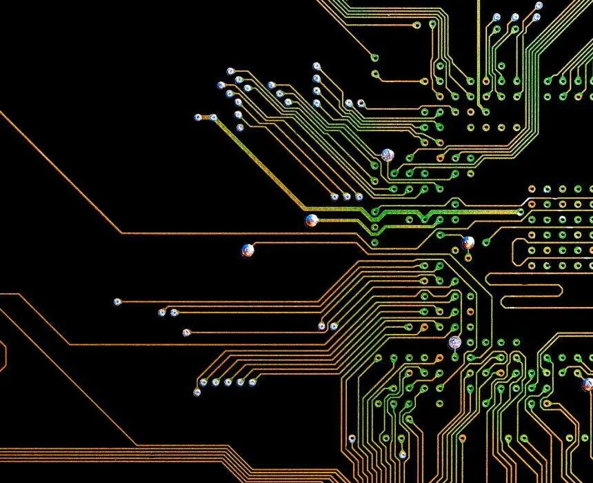
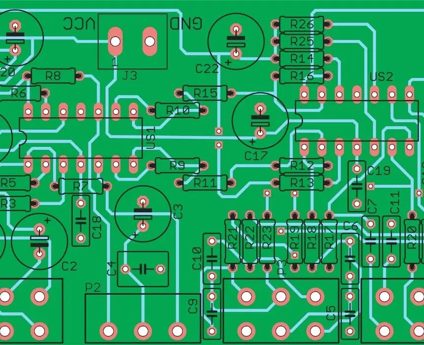
Challenge 1: Signal Integrity Failures That Look Like Firmware Bugs
Signal integrity is one of the most common PCB design challenges on first prototypes, and the hardest to distinguish from firmware problems. Engineers assume that if the schematic is correct, the signals will be correct. That assumption breaks down above 50 MHz, and high-speed PCB design issues become the dominant failure mode.
Impedance Mismatch Corrupts High-Speed Interfaces
When a signal trace has uncontrolled impedance, energy reflects back toward the source. On a USB 2.0 differential pair, that reflection closes the eye diagram at the receiver and the host controller rejects the device. On SPI at 20 MHz, it shows up as intermittent data corruption that looks exactly like a firmware bug.
Use controlled impedance routing for any interface above 50 MHz. Work with your PCB stackup to calculate the trace width that hits your target: typically 50Ω single-ended, 90Ω differential for USB, 100Ω for Ethernet. Use your EDA tool's impedance calculator, not a rule of thumb. Dielectric constant and copper weight both shift your numbers.
Broken Return Paths Radiate and Corrupt
Every high-frequency signal needs a return path directly beneath it in the reference plane. When you route a signal across a slot, gap, or split in the ground plane, you force the return current to detour. That detour creates a loop that radiates EMI and injects noise into every trace nearby.
Never route high-speed signals across plane splits. If a crossing is unavoidable, add a 100nF stitching capacitor at the crossing to give return current a low-impedance AC path.
Differential Pairs Demand Length Matching
For USB, LVDS, MIPI, and Ethernet, differential pairs must be length-matched within tight tolerances. A 50ps skew between D+ and D− on USB 2.0 is enough to fail compliance testing. Match differential pairs within 5 mils for USB 2.0 and within 2 mils for USB 3.0 or faster interfaces. Route them together from source to termination. Never split them around obstacles.
Interface | Impedance Target | Length Match Tolerance | Common Failure Mode |
|---|---|---|---|
USB 2.0 | 90Ω differential | ≤ 5 mils | Eye diagram closure, enumeration failure |
USB 3.0 | 90Ω differential | ≤ 2 mils | CRC errors, link training failure |
Ethernet 100M | 100Ω differential | ≤ 5 mils | Packet loss, auto-negotiation failure |
LVDS | 100Ω differential | ≤ 2 mils | Bit errors at high data rate |
MIPI CSI -2 | 100Ω differential | ≤ 1 mil | Camera data corruption, lane sync failure |
Challenge 2: Power Rail Noise That Destroys Analog Performance
Power integrity is a PCB design challenge most first-time hardware engineers underestimate. It's also the hardest to isolate, because noise on rails presents as analog problems or firmware behavior rather than a layout error.
Decoupling Placement Matters More Than Value
Decoupling capacitors work by storing charge locally and releasing it faster than your power supply can respond. But a 100nF capacitor placed 10mm from the IC it's meant to protect is largely useless. The trace inductance between them cancels most of the benefit before the capacitor can respond.
Place ceramic decoupling capacitors within 0.5mm of every VCC pin on every IC. Bulk capacitors (10µF–47µF) belong within 5mm of the power entry to each functional block. For ICs with switching edges above 500 MHz, add a parallel 10nF or 1nF high-frequency bypass capacitor on the same via. Smaller capacitors self-resonate at higher frequencies and handle fast transients that larger caps miss.
PCB layout best practices for decoupling on every board:
Place decoupling before routing signal traces. Never retrofit it around finished routing.
Use multiple smaller caps in parallel rather than one large one to reduce equivalent series inductance (ESL).
Keep vias for the decoupling cap between the cap and the IC pin, not on the far side.
Isolate analog power (AVCC) from digital power (DVCC) with an LC filter or ferrite bead.
LDO and Switcher Stability Requires the Right Output Cap
LDO regulators specify minimum and sometimes maximum output capacitor ESR. Use a capacitor outside that window and the LDO oscillates: producing a rail that looks stable on a bench multimeter but shows hundreds of millivolts of ripple on an oscilloscope. Check the datasheet. Use the recommended capacitor type and value, not whatever ceramic cap is already in your footprint library.
Challenge 3: EMI Failures That Show Up at Certification, Not on the Bench
EMI is a PCB design challenge engineers discover at the worst possible moment: during FCC Part 15 or CE pre-compliance testing, with a product launch already on the schedule. By that point, the fix requires a full board respin.
Large Loop Areas Are the Root of Most EMI Problems
Radiated emissions are proportional to loop area. Every signal and its return current form a loop. The larger the loop, the stronger the antenna. Keeping high-speed signal traces directly above a solid ground reference plane minimizes loop area, which is why a solid, uninterrupted ground plane is the single most effective PCB EMI interference solution available before any shielding or filtering.
Effective multilayer PCB design for EMI control follows this stackup logic:
Layer | Recommended Use | EMI rationale |
|---|---|---|
Layer 1 | Signal (short, controlled impedance) | Minimizes trace length |
Layer 2 | Solid ground plane | Return path directly under Layer 1 signals |
Layer 3 | Power plane | Shielded by ground on Layer 2 |
Layer 4 | Signal (less critical routing) | Sandwiched between planes |
For 6-layer and 8-layer boards, place a ground plane adjacent to every signal layer. This is the most reliable multilayer PCB design tip for first-pass FCC/CE compliance. It also eliminates one of the most expensive electronics design pitfalls teams face at the certification stage.
Via Stitching Closes the Gaps in Your Ground Plane
Ground stitching vias around the board perimeter and around RF sections prevent high-frequency noise from coupling between sections of the board. Space stitching vias at λ/20 of your highest frequency of concern. For a 2.4GHz BLE or Wi-Fi design, that means roughly 6mm spacing between stitching vias.
Every I/O Line Leaving the Board Is an Antenna
USB cables, power input wires, ribbon cables: anything that exits the PCB can carry noise in or out. Add common-mode chokes on differential I/O lines, ferrite beads on power entry, and TVS diodes on all external-facing pins. Most engineers skip these components to save BOM cost on the first prototype. Most add them back after failing EMC testing.
Challenge 4: Thermal Failures That Only Appear Under Real Operating Conditions
Thermal management is a board design issue that punishes optimism. Your prototype passes every functional test at room temperature. You put it in an enclosure at 40°C ambient and a component hits thermal shutdown 20 minutes later. Nothing in your bench test predicted it.
Exposed-Pad ICs Need Thermal Vias, Not Just Solder
QFN, DFN, and LGA packages dissipate most of their heat through the exposed pad on the bottom of the package. Without thermal vias through that pad to the ground plane below, the heat has nowhere to go. The laminate acts as insulation, and the die temperature climbs until the IC shuts down or fails permanently.
Standard practice: 0.3mm thermal vias on a 1.0mm–1.2mm grid under the exposed pad, connected to internal ground planes. For a 5mm × 5mm exposed pad, 9–16 thermal vias gives adequate thermal resistance reduction without creating solder wicking problems during reflow.
Challenge 5: PCB Design for Manufacturing Errors That Delay Production
DFM errors are circuit board design mistakes that don't kill your prototype. They kill your production timeline. A board that works perfectly as a hand-assembled prototype can be un-manufacturable at volume, adding weeks of delay and thousands of dollars in rework.
Common PCB design for manufacturing errors to catch before sending to fab:
Insufficient solder mask clearance. Mask opening too close to adjacent pads causes bridging during reflow. Check clearances against your assembly house's process capabilities per IPC-7351 guidelines, not generic default rules.
Missing or wrong polarity markers. Electrolytic capacitors, diodes, and polarized connectors need clear, visible polarity markings on the silkscreen. Markings covered by solder mask or pads are a production risk.
No test points. Every net that requires in-circuit testing or programming needs an accessible test point. Retrofit test points are always awkward. Plan them from the start.
Via-in-pad without fill. Vias inside SMD pads wick solder during reflow and cause tombstoning or insufficient joints. Either move the via out of the pad or specify filled and capped vias in your fab notes.
Component placement clearance. Pick-and-place machines need clearance around components for the nozzle to access them. Check your assembly house's minimum spacing requirements before you finalize placement.
Panel format not confirmed. Most assembly houses require boards panelized with V-score or tab-routed breakouts. Confirm your panel format and fiducial placement before you finalize the design.
DFM Issue | Consequence | Fix |
|---|---|---|
Via-in-pad (unfilled) | Solder wicking, weak joints | Specify filled/capped vias or move via off-pad |
Missing test points | Cannot test or program in production | Add test points to every critical net |
Tight component spacing | Pick-and-place nozzle collision | Maintain 0.2mm minimum between component bodies |
Wrong courtyard overlap | Assembly conflict | Run DRC courtyard check before Gerber export |
No fiducials | Poor optical alignment | Add 3 fiducials to every PCB panel |
Challenge 6: Schematic Errors That Pass DRC but Fail on the Board
Schematic-level mistakes are the PCB layout errors hardest to catch, because your EDA tool clears them with zero violations. DRC finds shorts and open nets. It doesn't find a pull-up resistor on the wrong voltage rail, a reset pin left floating when it should be tied high, or a bypass capacitor placed on a net that doesn't need it while the net that does is left unprotected.
Common schematic-level hardware design problems that survive DRC:
Reset and enable pins left floating. Most ICs require active drive on reset, enable, and chip-select pins. A floating pin means unpredictable behavior that changes with PCB revision, temperature, and board-to-board variation.
I2C pull-ups on wrong voltage rail. Pull-up resistors must reference the same voltage as the device with the lowest logic-high threshold on the bus. Mix a 3.3V MCU with a 1.8V sensor and you need level translation, not just pull-ups to the wrong rail.
Power sequencing not enforced. Many FPGAs, processors, and multi-rail ICs require power rails in a specific startup order. Violate the sequence and you risk latch-up, data corruption, or permanent component damage. Use an enable pin, sequencing IC, or RC delay to enforce the order.
Unused GPIO left floating. Floating pins on MCUs and FPGAs draw excess current, create noise susceptibility, and trigger spurious interrupts. Pull every unused GPIO to a defined logic state.
Hardware Design Review Checklist: What to Verify Before Sending to Fab
Use this pre-fab layout review before every Gerber export. It covers the PCB design challenges and board design issues that DRC misses: the layout and schematic decisions that only reveal themselves when current flows.
Signal Integrity
All high-speed traces use controlled impedance routing
No high-speed signals cross plane splits or gaps
Differential pairs are length-matched to tolerance
Series termination resistors placed at the driver output, not the receiver
Power Integrity
100nF decoupling capacitor within 0.5mm of every IC VCC pin
Bulk capacitor within 5mm of every power domain entry
AVCC isolated from DVCC with ferrite bead or LC filter
LDO output capacitor type matches datasheet specification
EMI and Ground
Ground plane is solid and uninterrupted under all high-speed signals
Ground stitching vias placed around board perimeter and RF sections
Common-mode chokes on all external-facing differential I/O
TVS diodes on all ESD-sensitive external pins
Thermal
Thermal vias under all exposed-pad packages
Tj calculated for all high-dissipation components at worst-case ambient
Copper weight specified for thermally critical layers
DFM
Via-in-pad reviewed; filled/capped specified where required
Test points on every net requiring in-circuit or production test
Polarity markers visible and not covered by solder mask
Component courtyard overlap DRC passes with zero errors
Fiducials placed on panel
Common Questions Engineers Ask Before Their First PCB Spin
What causes most first-prototype PCB failures?
Most prototype board failures trace back to three root causes: poor ground plane continuity that creates noise and EMI, missing or misplaced decoupling capacitors that allow power rail instability, and uncontrolled impedance routing on high-speed interfaces that corrupts signals before they reach the receiver. These PCB design challenges are invisible in schematic review and invisible to DRC. They only appear when current flows through the board.
How do I know if my PCB has a signal integrity problem?
PCB signal integrity problems typically show up as intermittent communication failures, eye diagram violations on high-speed interfaces, or data errors that vary with temperature or board orientation. Scope the signal at both the driver output and the receiver input. If the waveform looks clean at the driver but degraded at the receiver, with ringing, overshoot, or slow edges, you have an impedance or routing problem. If both ends look degraded, the fault is likely power integrity or ground noise.
What is the most common PCB EMI problem and how do I fix it?
The most common EMI problem is a broken or discontinuous ground plane that forces return currents to take long paths, creating loop antennas. Keep your ground plane solid and uninterrupted under all high-speed signal layers. Add via stitching around the board perimeter and RF sections. Filter every I/O line that exits the board with common-mode chokes or ferrite beads. Most boards that fail FCC Part 15 or CE emissions testing have at least one of these three issues.
When should I use multilayer PCB design versus a 2-layer board?
Use 2-layer boards only for simple, low-speed designs with minimal analog content and no RF. Move to a 4-layer stackup when you have any interface above 25 MHz, any precision analog circuitry, any RF subsystem, or any IC with an exposed thermal pad requiring thermal vias. The cost difference between 2-layer and 4-layer fabrication is small. The debug time saved by having dedicated ground and power planes is substantial, and for most IoT and connected hardware products, 4 layers is the practical minimum.
How do I prevent PCB design for manufacturing errors before sending to fab?
Run DFM review against your assembly house's specific design rules, not the generic defaults in your EDA tool. Key checks: via-in-pad requires filled vias, component spacing must meet pick-and-place nozzle clearance, every net needing production test needs a test point, and your panel must have fiducials. Send a preliminary design to your assembler for DFM feedback before finalizing. Most assemblers offer this at no cost, and it prevents expensive rework.
How many PCB layers do I need for a BLE product?
Most BLE products achieve adequate RF performance on a 4-layer stackup with a solid Layer 2 ground plane. The critical requirements are a solid, uninterrupted ground plane beneath the antenna area, via stitching around the RF section, and the antenna kept clear of copper pours on adjacent layers. For certified antenna modules — u-blox NINA, Nordic nRF52840, or similar — follow the vendor's reference layout exactly. Deviating from it voids the RF certification and restarts your compliance process from scratch.
What to Do When Your First Board Comes Back Broken
Start with the power rails. Probe them with an oscilloscope while the board runs under load. Look for ripple above 50mV peak-to-peak on any rail feeding analog or RF circuits. If the rails are clean, scope the failing interface and compare the waveform to the device's electrical specifications.
Clean rails and clean signals with a firmware failure is a firmware problem. Noisy rails or degraded signals with what looks like a firmware failure is almost always a board bring-up issue rooted in layout.
PCB design challenges are fixable. Almost all of them fixable before fabrication, with a systematic layout review against the checklist above. The engineers who ship boards that work on the first spin aren't luckier. They check the same things every time, before every tape-out.
If you're working on a hardware product and want a second set of eyes on your PCB layout before it goes to fab, CoreFragment's hardware team has reviewed and corrected board designs for medical devices, industrial systems, and IoT products and can tell you exactly what to fix before you spend money on a prototype spin.
Author
Have Something on Your Mind? Contact Us : info@corefragment.com or +91 79 4007 1108
Related articles

_title.webp)