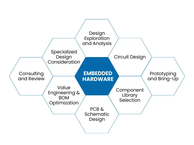
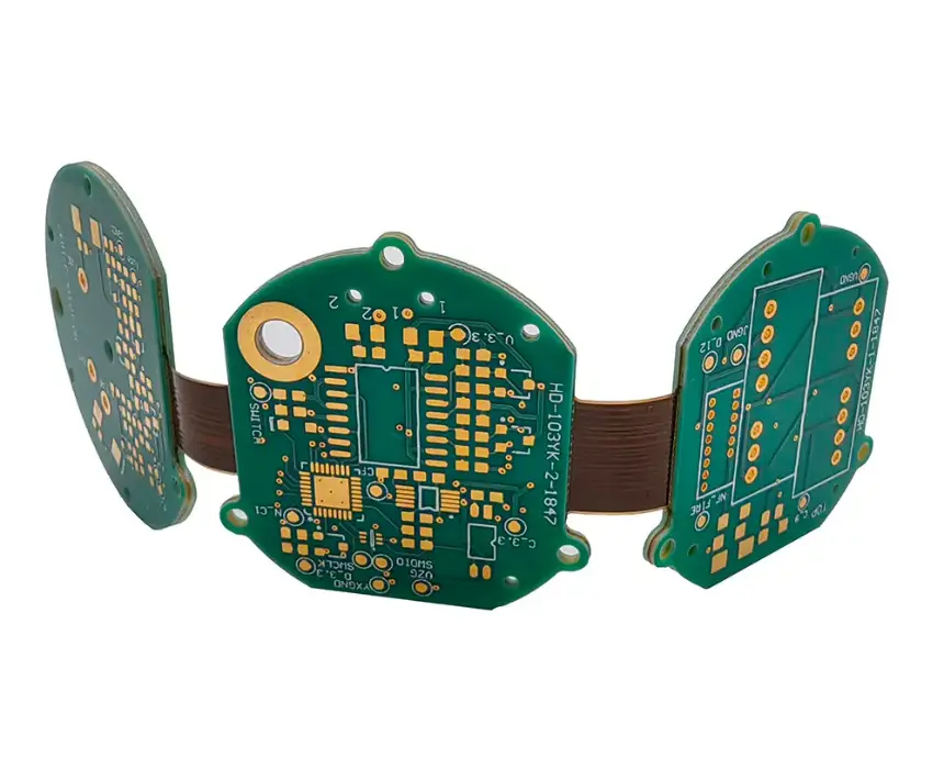
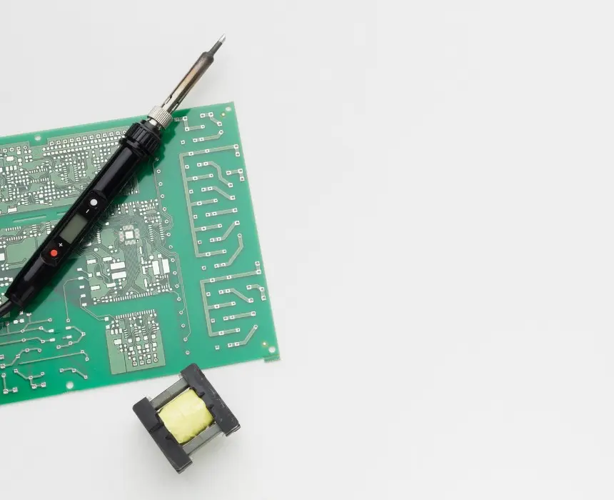
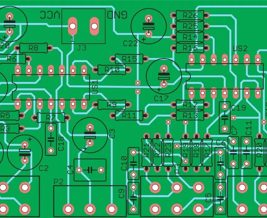
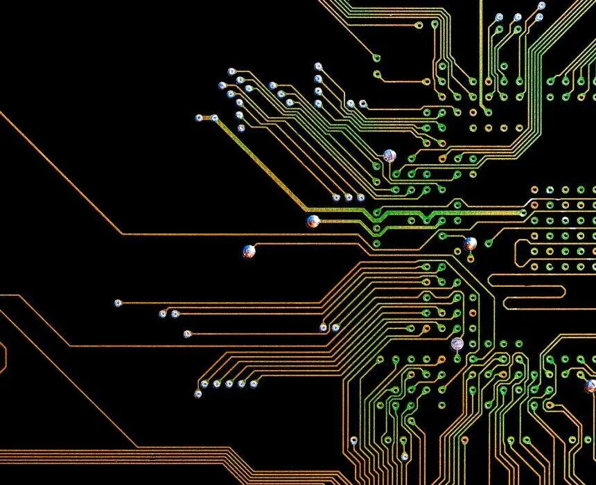
Our embedded hardware development services include PCB design, schematic creation, and board bring-up. We design multilayer PCBs with high-speed signals, power distribution, and EMI considerations. From prototype to production, we deliver hardware that integrates with your firmware smoothly.
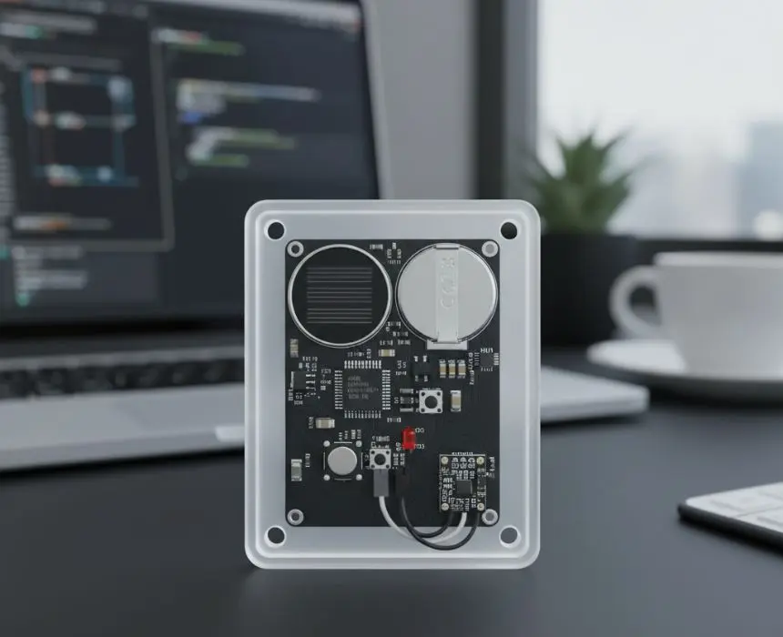
As a hardware engineering company, we handle component selection, BOM optimization, and manufacturing support. Our engineers design analog circuits, digital interfaces, and power management systems. We have delivered custom boards across medical device, wearables, industrial automation.
We specialize in mixed-signal PCB design, RF circuit layout, and signal integrity analysis. Your product needs hardware engineered for scalability and reliability. We provide complete design files, test procedures, and hardware documentation with Gerber files ready for fabrication.

Our hardware engineering work spans the full product lifecycle. These are the specialist services our clients bring us in for alongside or independent of a full design engagement.
We design schematics with production in mind - selecting components based on technical fit, cost, availability, and long-term supply chain stability. We verify MCU peripheral pinouts against firmware requirements, confirm power sequencing, and run design rule checks before a single copper trace is placed. Every schematic is handed over in a documented, maintainable format with full BOM including second-source options and lifecycle status for every key component.
Validation is what separates a prototype from a product. We run functional verification tests across operating conditions, measure power consumption against your budget, perform signal integrity measurements on high-speed interfaces, and conduct environmental stress testing where your application requires it. Test results are documented in validation reports formatted for CE, FCC, and IEC certification submissions - so your regulatory team has what they need without chasing us for data.
Power subsystem failures account for a disproportionate share of hardware field returns. We design power trees from input protection through LDO and switching regulators to load distribution — with correct sequencing, soft-start, and fault protection at every stage. For battery-powered products we handle battery management IC selection, fuel gauge integration, charge control circuitry, and overcharge, over-discharge, and short-circuit protection tested to IEC 62133 requirements.
A BOM that looks fine on paper can quietly kill a product through single-source components, end-of-life parts, long lead times, or unit costs that do not survive volume pricing negotiations. We audit every component on your BOM for technical fit, lifecycle status, second-source availability, and cost at your target production volume. Where we find risk, we identify qualified alternates that meet or exceed the original specification. We also work with your procurement team or preferred distributors to validate pricing, confirm stock positions, and reduce BOM cost without compromising performance or reliability.
PCB antenna design, RF trace routing, and antenna placement review for BLE, Wi-Fi, LoRa, LTE-M, GPS, and UWB applications. We model antenna performance relative to your enclosure geometry and nearby ground planes, select or design antenna geometry for your form factor constraints, and verify performance with network analyser measurements on prototype hardware before the design goes to certification testing.
Pre-compliance EMI/EMC scanning, documentation preparation, and engineering support for CE, FCC, UL, IEC, and industry-specific certification programs. We prepare test plans, resolve failing tests at the schematic and layout level rather than through shielding and filtering workarounds, and produce the technical file documentation your notified body requires — including Declaration of Conformity, technical construction file, and risk assessment where applicable.
We do not hand over Gerber files and disappear. Every board we design is engineered to pass validation, survive its operating environment, get through certification, and be manufacturable at the cost your product needs.
A design built around a single-source component or an EOL part is a liability. We select components with second-source availability, check lifecycle status, and flag anything with constrained supply before the BOM is finalised, so you do not discover the problem six months into production.
We route components for pick-and-place accessibility, select packages your CM can source, and verify pad geometry against IPC standards before we release any design for fabrication. Our designs do not get sent back from the CM with a list of assembly queries.
Hardware and firmware designed in isolation produce integration problems that cost weeks to resolve. Our hardware engineers work directly with the firmware team — verifying that peripheral pinouts match driver requirements, that debug interfaces are accessible, and that the memory map makes sense before layout begins.
Your hardware design is your IP. We sign a mutual NDA before any technical discussion. You receive the complete design package from schematic source files, PCB project files, Gerbers, BOM, assembly drawings, and validation reports. We retain nothing.
We offer embedded software, app development, IoT and AI development services as we are full stack product engineering company.
We develop custom IoT firmware, OTA integration, linux and RTOS based development, BSP development, hardware-firmware integration, kernel and bootloader development.
More DetailsWe develop custom mobile app in IoT, wearables, healthcare in android, iOS and cross platform.
More DetailsWe develop custom web app for industries like healthcare, manufacturing, consumer electronics products etc.
More DetailsWe follow a structured, milestone-driven hardware development process from the first requirements call to manufacturing handover. Every phase has clear deliverables and sign-off before the next begins.
1
We go through your product concept, performance requirements, target BOM cost, form factor constraints, connectivity needs, and regulatory certification targets. We come out of that call with a shared understanding of what we are building and why.
2
We define the hardware architecture - processor selection, memory configuration, power tree topology, connectivity stack, and interface requirements. We document everything in a Hardware Requirements Specification reviewed and agreed with your team before schematic work begins.
3
We design the full schematic, select components with BOM cost and supply chain health in mind, and run a formal design review before layout. Your team is involved in the review.
4
Layout proceeds with impedance targets, stackup specification, and EMI mitigation strategy agreed upfront. We run signal integrity and power integrity analysis on critical nets before submitting Gerbers. You receive a full layout review package and not just fabrication files.
5
We manage fabrication and assembly, then work through board bring-up in our lab. Power rails, clocks, debug interfaces, and peripherals are validated in sequence. Bring-up issues are documented and resolved. You receive a working, characterized prototype with bring-up notes.
6
We run functional, environmental, and pre-compliance tests. We produce the full manufacturing handover package — Gerber files, BOM, assembly drawings, test procedures, and validation reports. Your CM gets everything needed to start production without calling us for missing files.


We design 2-layer through 16-layer boards. rigid, flex, and rigid-flex - depending on the complexity, signal count, and form factor requirements of your product. Simple sensor nodes often work well on 4-layer boards. High-speed processor designs with DDR memory, Ethernet, and USB 3.0 typically need more than 6 layers.
Our hardware development service covers the full design cycle. Hardware architecture definition, schematic capture, component selection, PCB layout, DFM-DFA analysis, prototype fabrication management, board bring-up, functional validation, pre-compliance EMI testing, and manufacturing handover.
es, always. We sign a mutual NDA before any technical discussion begins. Your product concept, hardware architecture, BOM, and IP are fully protected throughout the engagement. All design files, documentation, and test data are transferred to you at project completion. We retain no copies and make no claim to your IP.
Yes. Our embedded software team works alongside our hardware engineers throughout the process . Aligning hardware parameters with firmware requirement before layout begins. Clients who use both services reach a working hardware-firmware system faster than those who manage the separate vendors for hardware and firmware.
Yes ,component selection is a core part of our service, not an afterthought. We select components based on technical fit, unit cost, package availability, second-source options, and lifecycle status. We flag any single-source or end-of-life parts before the BOM is finalised.