- May 28, 2026
Summarize with AI
Not enough time? Get the key points instantly.
Get summary:
Why Wearable PCB Checks Before Sending Gerber Files to Production is Important?
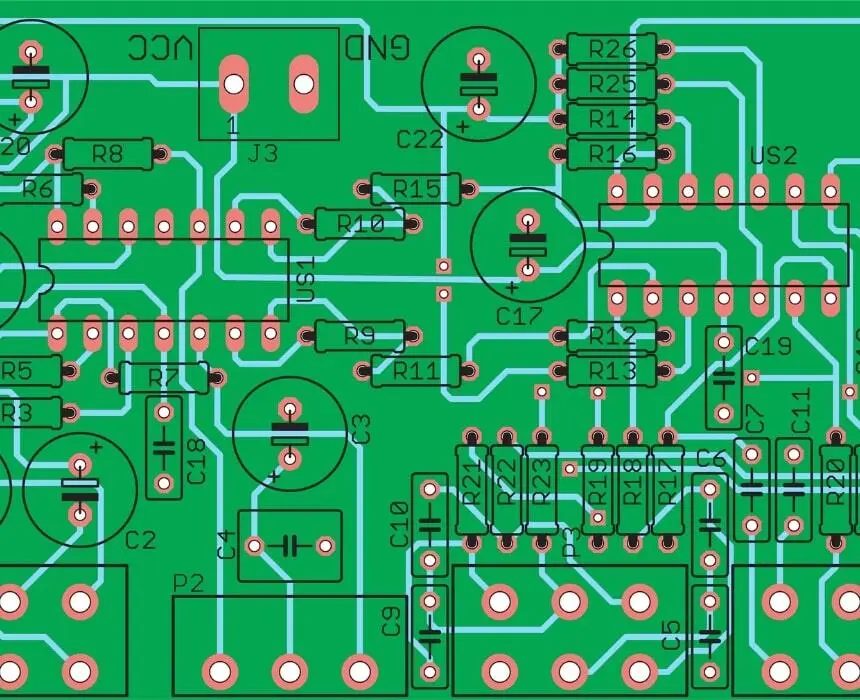
The PCB layout looks complete. The schematic passed review. The design rule check shows zero errors. The natural next step is to export Gerbers and send them to the fab.
Wait. Not yet.
A wearable PCB that passes DRC and looks correct on screen fails in specific, expensive ways. All of them show up on physical hardware, after a four-week fabrication and assembly cycle. BLE range drops to 3 metres. Antenna ground plane not cleared. The PPG sensor reads noise instead of pulse because a switching regulator was routed too close to the photodetector. The device resets under load because the power rail has a ground plane split that nobody noticed on the schematic.
By the end of this post, you will know every check that experienced wearable hardware teams run before Gerbers leave the building, and why each one matters specifically for a body-worn device rather than a standard IoT design.
Why Wearable PCB Design Guidelines Differ From Standard PCB Rules
Standard PCB design rules exist for benchtop electronics. Wearable PCB design guidelines start from different assumptions entirely. They assume fixed geometry, controlled temperature, and a known RF environment. A wearable violates all three assumptions.
The body changes everything.
A wearable PCB sits against skin. Inside a curved enclosure. On a moving limb. The rules are different. The human body is a conductor at RF frequencies. It absorbs BLE signals. It introduces parasitic capacitance on sensing electrodes. It changes the effective dielectric constant of the PCB substrate at the antenna region. It radiates heat into the PCB. None appear in DRC. All show up on a person. All of them affect whether the device works on a person.
Three failure modes that DRC cannot catch:
Antenna detuning from body proximity : A BLE antenna tuned correctly on a bench becomes detuned when placed against a wrist. The human body shifts the antenna's resonant frequency. A design that does not account for this produces a device with good bench range and poor real-world range. The fix — a keep-out region under the antenna plus body-adjacent tuning happens at layout time, not after fabrication.
Optical sensor contamination from switching noise : A PPG optical sensor is measuring changes in reflected light at the picoamp level from the photodetector current. A switching regulator placed near the optical sensor couples switching noise into the photodetector signal. This noise appears in the PPG waveform as artifacts that the firmware cannot distinguish from real signal. The fix is routing, placement, and shielding, not firmware.
Mechanical failure from wear stress : A wearable PCB flexes, vibrates, and experiences impact events that a benchtop board never encounters. Via cracks, solder joint fatigue, and connector wear patterns are the most common causes of field returns on wearable products. None of these appear in DRC because they are mechanical failure modes, not electrical ones.
BLE Antenna Guidelines: The Most Commonly Violated Rule on Wearable PCBs
BLE antenna performance on a wearable is one of the most common first-revision failures. The cause is almost always one of four layout decisions that look correct on screen but fail on hardware.
Rule 1: Clear the antenna keep-out zone completely
Every BLE antenna (chip antenna, PCB trace antenna, or external antenna module) has a keep-out zone specified in the component datasheet or antenna manufacturer's application note. This zone must contain no copper on any layer, no vias, and no ground plane fill. Any copper within the keep-out zone detunes the antenna and reduces range.
The most common violation: a ground pour that floods to the edge of the PCB and overlaps the keep-out zone on the bottom layer. It looks like a ground pour filling unused space. It drops BLE range from 10 metres to 2 metres.
Rule 2: Place the antenna at the PCB edge, facing away from the body
The antenna radiates from its tip or along its length depending on the antenna type. On a wearable, the antenna should face away from the body. Towards the air, not towards the skin. Placing the antenna on the body-facing side of the PCB means the human body absorbs a significant portion of the radiated power.
Position the antenna at the edge of the PCB, on the side that faces outward from the enclosure when the device is worn. This cannot be corrected after layout without a revision.
Rule 3: Do not route any signals under or near the antenna
Signal traces running under the antenna coupling region act as parasitic elements that affect antenna impedance. Power traces are worse because they carry switching noise. The area directly beneath and adjacent to the antenna should be empty on all layers except the antenna feed network itself.
Rule 4: Match the antenna feed impedance at 50 ohms
The transmission line from the MCU RF output to the antenna must be impedance-matched to 50 ohms. On a two-layer PCB, a 50-ohm microstrip trace width depends on the substrate height and dielectric constant. Typically 2 to 3mm wide on FR4 at 1.6mm thickness. A trace that is too narrow or too wide produces impedance mismatch, reflects power back into the RF output, and reduces both radiated power and receiver sensitivity.
BLE Antenna Mistake | Consequence | When Discovered |
|---|---|---|
Ground pour inside keep-out zone | Range drops to 2–3 metres | First outdoor test |
Antenna facing body | Range asymmetric, poor in-use | First wear test |
Signal traces under antenna | Impedance mismatch, reduced sensitivity | RF characterisation |
Wrong trace width on RF feed line | Reflected power, reduced range | RF characterisation |
No antenna matching network footprint | Cannot tune after fabrication | First range test |
PPG Sensor Layout Guidelines: Protecting the Optical Signal
A PPG optical sensor measures reflected light changes in the range of microamps or less from the photodetector output. At that signal level, the PCB layout determines whether the measurement is clean or noise-dominated. Firmware cannot fix a contaminated optical signal.
Placement rules:
The optical sensor must be on the body-contact side of the PCB, positioned directly against skin when the device is worn. Even a 0.5mm air gap reduces signal amplitude significantly. The enclosure must hold the sensor against the skin with controlled pressure. Not too loose. Not too tight.
The LED and photodetector must be positioned with a light barrier between them. Direct LED light reaching the photodetector without passing through tissue is noise. Not signal. The barrier (typically a dam of opaque silicone or a shielded PCB land) must extend from the PCB surface through the optical window.
Routing rules:
LED current traces carry high pulsed currents: typically 5 to 50mA in microsecond pulses. These traces must be routed away from the photodetector amplifier input and the analog-to-digital conversion circuitry. The photodetector input is the highest-impedance node on the PCB. Any current switching nearby couples noise into that node.
Route LED current on the opposite side of the PCB from the photodetector input when the stackup allows it. If both must be on the same layer, maintain maximum physical separation and place a ground shield trace between the LED current path and the photodetector input.
Power supply rules:
The optical sensor supply rail must be filtered at the point of entry to the sensor domain: a ferrite bead followed by a small decoupling capacitor. Switching noise from the MCU power domain or BLE radio couples through the supply rail into the optical signal path. A clean supply rail is the first line of defense against optical noise artifacts.
On one health wearable project, the first prototype showed a 60Hz artifact in the PPG signal that matched the switching frequency of the display backlight driver. The optical sensor supply and the display supply shared the same voltage rail. Adding a pi filter on the optical sensor supply and routing the display current traces away from the photodetector region eliminated the artifact entirely on the second revision.
Grounding Guidelines: The Layout Decision That Affects Everything
Ground plane design on a wearable PCB determines signal quality for analog sensors, RF performance for the wireless antenna, and EMC compliance for regulatory testing. A ground plane error is one of the hardest problems to fix without a layout revision.
Keep the analog and digital ground planes separate and joined at one point
Analog sensors (optical sensors, bioimpedance electrodes, temperature sensors) need a quiet ground reference. Digital circuitry (MCU, BLE radio, switching regulators) generates ground noise from current switching. If analog and digital circuitry share the same ground path, digital noise couples into the analog measurement.
On a wearable PCB, separate the analog and digital ground planes with a slot or gap, and connect them at a single star point near the power supply. Current from the digital domain returns to the power supply through the digital ground path without crossing the analog ground plane.
Never split the ground plane under the antenna
A ground plane split under or near the antenna creates an impedance discontinuity in the antenna ground reference. This shifts the antenna resonant frequency and changes the radiation pattern. Even a slot intended to separate analog and digital ground must not pass through the antenna region.
Fill unused copper with ground pour on all inner layers
On multi-layer wearable PCBs, fill unused areas of inner layers with ground copper connected to the main ground plane through vias. This reduces ground impedance, improves RF shielding, and reduces susceptibility to interference. Floating copper islands (pours not connected to anything) must be identified and removed. They act as unintended antennas.
Via placement near sensitive nets
Ground vias placed too close to high-impedance sensor inputs create capacitive coupling paths between the ground plane and the signal net. Keep ground vias at least 0.5mm from any analog signal net. For optical sensor circuits, increase this clearance to 1mm or more.
Mechanical and Reliability Guidelines Specific to Wearable PCBs
A wearable PCB endures mechanical stresses that benchtop electronics never experience. The mechanical guidelines below address the failure modes that cause the most field returns on wearable products.
Connector placement and strain relief
The charging connector is the highest-stress mechanical interface on any wearable. It receives insertion and removal forces multiple times per day for the product lifetime. Place the charging connector at the PCB edge with a mounting pad configuration that distributes pull-out force across multiple pads rather than concentrating it at the connector body.
Add mechanical strain relief to all cable connections inside the enclosure. A wire soldered directly to a PCB pad without a strain relief point will fatigue and break at the solder joint within weeks of regular use. The strain relief is a design element, not an assembly afterthought.
Via design for mechanical durability
Vias in wearable PCBs experience thermal and mechanical cycling from daily wear. Microvias and buried vias are more mechanically reliable than through-hole vias on a thin PCB that sees flex stress. Tented vias (covered by soldermask) are more resistant to mechanical damage than open vias during handling and wear.
Avoid placing vias in high-stress regions: at the battery connector footprint, at the charging connector, and at any point where the PCB is clamped or screw-mounted into the enclosure. Via cracking at these locations is a common cause of intermittent failures in deployed wearable devices.
Component placement for drop resilience
Heavy components (batteries, large capacitors, connectors) placed near PCB edges experience higher stress during drop events. Heavier components should be placed toward the centre of the PCB or supported by the enclosure on both faces. Components near unsupported PCB edges are at higher risk of pad delamination during drop impact.
Conformal coating on the PCB after assembly adds significant moisture and mechanical protection for a wearable device that will encounter sweat. The coating must not cover the optical sensor window or any test points used during production testing.
Wearable PCB Design Guidelines Checklist: Run Before Sending Gerbers
BLE antenna:
Keep-out zone is clear of all copper on all layers — check bottom layer pour separately
Antenna positioned at PCB edge on the non-body-facing side
No signal or power traces routed under or adjacent to the antenna region
RF feed line width matches 50-ohm impedance for the PCB stackup
Matching network footprint included — populated with zero-ohm if not needed but available for tuning
PPG optical sensor:
Sensor on body-contact side, positioned for consistent skin contact in the enclosure
Light barrier between LED and photodetector confirmed in layout and enclosure design
LED current traces routed away from photodetector input net
Optical sensor supply has ferrite bead and decoupling filter at domain entry
Ground shield trace between LED current path and photodetector input where same-layer routing is unavoidable
Grounding:
Analog and digital ground planes separated and joined at single star point
Ground plane split does not pass through antenna region
All inner layer copper fills connected to ground through vias — no floating copper islands
Ground vias maintain 0.5mm minimum clearance from all analog signal nets
Mechanical reliability:
Charging connector has distributed mounting pads and PCB-edge placement
All internal cable connections have mechanical strain relief designed in
Vias avoided in high-stress mechanical zones: connector footprints, screw mounts, battery clamp
Heavy components placed toward PCB centre or supported by enclosure on both faces
Conformal coating specified for production build, with masking requirements documented
Frequently Asked Questions
How long does it take to do a proper design review before sending wearable PCB Gerbers?
A structured pre-Gerber review on a wearable PCB typically takes 4 to 8 hours for an experienced wearable hardware engineer. This covers antenna placement and keep-out verification, sensor layout and routing audit, power rail noise path analysis, ground plane integrity check, and mechanical stress point review. For a first-time wearable design where the layout engineer does not have wearable-specific experience, the review frequently identifies 3 to 6 issues that would otherwise produce a revision. Spending 8 hours in review before Gerbers is faster than spending 4 weeks waiting for boards that will need to be revised.
What is the most common layout mistake that causes a wearable PCB to need a second revision?
Antenna keep-out violation is the most common cause of an unnecessary revision. It is easy to introduce because ground plane flooding is applied as a final step after routing, and the automatic pour algorithm fills to the DRC-defined minimum clearance. That is an electrical clearance, not an RF clearance. The RF keep-out zone is defined in the antenna datasheet or application note, not in the PCB tool's electrical rules. Most designers who have not worked with antenna placement before do not check it explicitly. The result is a device with BLE range that fails the specification by a wide margin, requiring a layout revision and another fabrication cycle.
Should I use a rigid-flex PCB or a rigid PCB for a wrist-worn wearable device?
Use a rigid PCB for first and second revisions unless the form factor requires flexibility. Rigid PCBs are faster to fabricate, easier to assemble, and simpler to prototype. Rigid-flex adds cost, longer lead times, and complexity that is unnecessary until the form factor is stable. Move to rigid-flex when the mechanical design is finalised and the PCB layout will not change significantly. Introducing rigid-flex on a first revision that will require multiple layout changes is expensive. Each revision requires a new rigid-flex stack and potentially a new enclosure iteration.
How does the human body affect BLE performance on a wearable PCB?
The human body absorbs RF energy at 2.4GHz and shifts the resonant frequency of nearby antennas. A BLE antenna optimised in free space typically shows 5 to 10dB of additional path loss when placed against a wrist compared to a bench measurement. For a wearable that needs reliable BLE connectivity at 5 to 10 metre range, the antenna must be tuned for on-body conditions, not bench conditions. This requires either an antenna type designed for on-body use or a post-fabrication tuning step using a network analyser with the device worn. Teams that tune only on the bench produce devices with poor real-world BLE performance.
How much does a wearable PCB design revision cost and how long does it take?
A wearable PCB design revision — schematic update, layout revision, DFM review, Gerber export, fabrication, and assembly — typically costs between USD 2,000 and 8,000 and takes 5 to 8 weeks from decision to tested boards. The cost depends on board complexity, assembly component count, and whether any new components are introduced that require new footprints or updated BOMs. The timeline is dominated by PCB fabrication (5 to 10 business days for standard lead time) and assembly (5 to 10 business days depending on component availability). Finding and correcting a layout issue before Gerbers are sent costs a fraction of one revision. Finding it after costs one full revision cycle.
Does conformal coating affect sensor accuracy on a wearable PCB?
Conformal coating over the PCB protects against moisture and improves mechanical durability. It must be applied carefully around optical sensors and skin-contact electrodes. Coating over the optical sensor window blocks or attenuates the light path, reducing signal amplitude and introducing optical artifacts. Coating over bioimpedance or ECG electrodes increases contact impedance and degrades signal quality. The coating process must include masking specifications that document which areas must remain uncoated. Any change to coating coverage or material after the first production build must be validated against sensor performance. Coating formulation affects both optical transmission and skin contact impedance.
Conclusion
A wearable PCB that passes DRC and looks correct on screen can still fail in four different ways the first time it is worn by a real person. Wearable PCB design guidelines exist because BLE detunes by body proximity. Optical noise from a poorly routed switching supply. Ground splits that contaminate the sensor reference. Mechanical fatigue at the connector that shows up after three weeks of daily use.
The wearable PCB design guidelines in this post address each failure mode before it reaches fabrication. Run the wearable PCB design guidelines checklist before Gerbers leave. The antenna keep-out check takes 10 minutes. The optical sensor routing audit takes 20 minutes. Finding either issue after boards arrive costs four weeks.
If you are designing a wearable PCB and want a hardware team that runs this review as standard practice on every project, CoreFragment's embedded hardware team has designed wearable PCBs for health monitoring devices across consumer, clinical, and research applications. Share your layout and your sensor stack and you will get a direct assessment of what needs to change before you send Gerbers.
Author
Have Something on Your Mind? Contact Us : info@corefragment.com or +91 79 4007 1108

Related articles